Microfab Capacitors
Fall 2016
The objective of this lab was to develop an understanding of microfabrication and thin film deposition techniques including wafer cleaning and handling, PECVD deposition, RIE (etching), and lithographic patterning.
This understanding was applied to create a 5x5 array of MIS (metal-insulator-semiconductor) capacitors with 5 diameters ranging from 200 μm to 500 μm.
Devices were characterized using manual probe station equipped with parametric analyzers and precision source-measurement units (for I-V and C-V measurements), as well as an ellipsometer and DEKTAK (for thickness a surface profile characterization, respectively).
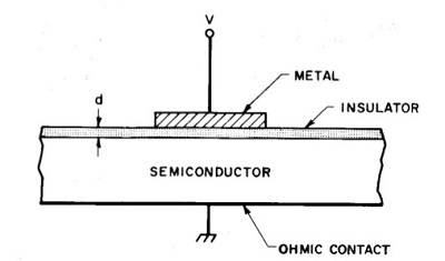
According to the ellipsometer, the thickness, d of the SiN dielectric of our capacitors were measured to be ~100-200 nm. These values were in agreement with similar thickness approximations using a DEKTAK stylus profiler and color chart.
The capacitance of the smallest capacitors (200 μm in diameter) peaked at roughly 25 pF, whereas the largest 400 μm capacitors reached capacitances closer to 50 pF. Most of the variance in capacitance for devices with the same diameter could be explained by thickness of the deposited film not being perfectly uniform.